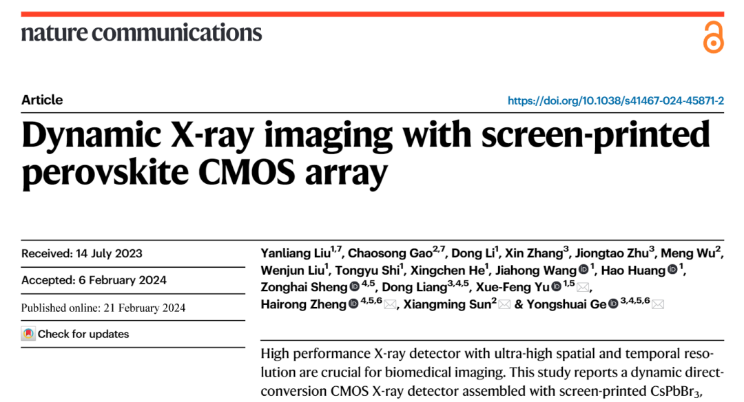
Nature Communications | Screen printed perovskite CMOS array detector achieves high-performance dynamic X-ray imaging
Recently, the Shenzhen Institute of Advanced Technology of the Chinese Academy of Sciences cooperated with Central China Normal University to publish the research paper "Dynamic X-ray imaging with screen printed perovskite CMOS array" online in the authoritative journal Nature Communications. After more than two years of joint research and development, the team has successively solved a series of key challenges such as the growth kinetics of perovskite semiconductor crystals, specialized low dark current CMOS pixel chips, data readout and image post-processing, and finally successfully developed a high-resolution, low-dose perovskite direct conversion X-ray detector based on CMOS pixel chips for the first time internationally.
Yu Xuefeng and Zheng Hairong, researchers of the Chinese Academy of Sciences Shenzhen Institute of Advanced Technology, Sun Xiangming, professor of Central China Normal University, Ge Yongshuai, researchers of the Chinese Academy of Sciences Shenzhen Institute of Advanced Technology, are the co corresponding authors of this article, and Liu Yanliang, associate researcher of the Chinese Academy of Sciences Shenzhen Institute of Advanced Technology, and Gao Chaosong, associate professor of Central China Normal University, are the co first authors of this article.

Online screenshot of the paper
Paper link: https://doi.org/10.1038/s41467-024-45871-2
X-ray detection and imaging are widely used in biomedical, industrial testing, and security inspection fields. The current commercial indirect conversion X-ray detectors using scintillators (such as cesium iodide) have technical bottlenecks such as low secondary photoelectric conversion efficiency and limited spatial resolution, which cannot meet the needs of high-end medical imaging and precision industrial detection. In contrast, direct conversion X-ray detectors based on semiconductor materials only require one photoelectric conversion to directly convert X-rays into electrical signals, with higher photoelectric conversion efficiency and spatial resolution, making them the forefront of the development of the next generation of high-end X-ray detectors.
In recent years, perovskite semiconductors have attracted much attention in the field of direct conversion X-ray detection due to their excellent optoelectronic properties. This research work innovatively developed a liquid-phase screen printing process. By dynamically controlling the growth and crystallization process of perovskite crystals, a perovskite semiconductor photosensitive layer was directly grown in situ on a CMOS chip, resulting in a thickness controllable, dense, uniform, and excellent optoelectronic properties of the perovskite photosensitive layer. The product of material mobility and lifetime reached 5.2 10-4 cm2 V-1, and the X-ray detection sensitivity reached 1.6 104 C Gyair-1 cm-2. The CMOS chip continuously scans samples vertically and horizontally at a frequency of 300 frames per second, achieving large-area projection imaging (size ≥ 5cm 10cm) and tomographic imaging of samples such as mouse and chicken leg tissues. Compared to traditional indirect conversion CMOS detectors, experimental results show that this new perovskite direct conversion CMOS detector is expected to reduce radiation dose by more than 50% while maintaining excellent spatial resolution (5.0 lp mm-1).
This work has significant characteristics of the intersection and integration of basic research and applied research, providing technical support for breaking the long-term technology blockade and monopoly of foreign countries and developing the next generation of high-performance X-ray detectors with independent intellectual property rights.
Direct conversion of perovskite into CMOS detectors and high-resolution, low-dose biomedical imaging results.
This research work has been funded by Shenzhen Key Basic Research Project, National Natural Science Foundation of China Key Project, Chinese Academy of Sciences Key Laboratory of Medical Imaging Science and Technology System (National), National High Performance Medical Device Innovation Center and other institutions.